A grand family of two-dimensional (2D) materials and their heterostructures have been widely applied in flexible sensors, photodetectors, high-frequency electronics, solar cells, data storage, low-power neuromorphic computing and ubiquitous electronics for their wide band gap selection, no dangling bonds, excellent mobility at atomic layer thickness, and high light absorption. These pioneering works contribute to realizing the fundamental platforms to explore and analyze new physical/chemical properties and technological phenomena at the micro–nano scales.
Recently, a paper entitled “2D Heterostructures for Ubiquitous Electronics and Optoelectronics: Principles, Opportunities, and Challenges” with the IF 60.6, written by by the research team of YU Bin, XU Yang and the team of DUAN Xiangfeng of the Future Science Research Institute at ZJU-Hangzhou Global Scientific and Technological Innovation Center was published on Chemical Reviews. Chemical Reviews is one of the top academic journals in the field of international chemistry and chemical engineering as well as the most authoritative review journal of American Chemical Society. Its 2020 impact factor released in 2021 was 60.6.
With an elaboration of the latest progress in the representation of 2D materials, the review focuses on the great impact of preparation methods, characterization techniques and physical parameters on 2D heterostructures. The main emphasis is on 2D heterostructures and 3D-bulk (3D) hybrid systems exhibiting intrinsic quantum mechanical responses in the optical, valley, and topological states as well as the application and development of 2D heterostructures in future electronics and optoelectronics.
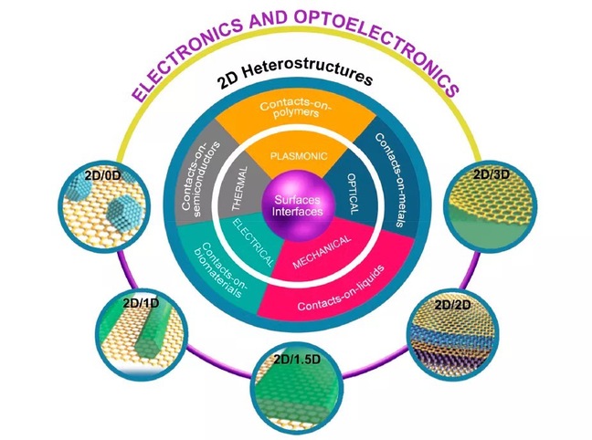
Surfaces/Interfaces of 2D Heterostructures and Materials of Different Dimensions
01. Characteristics and challenges of 2D Heterostructures
2D heterostructures are eessential to advancing the R&D of future electronics and optoelectronics, as they provide fundamental tools for exploring valleytronics, spintronics, and neuromorphism. However, the instability of the bonds on the surface of van der Waals nanoheterostructures restricts its extensive development and is in need of further in-depth research by researchers.
Currently, 2D heterostructures have not yet developed large-scale fabrication and integration technologies that match existing silicon processes. There are still grave challenges in material synthesis, device fabrication, and integration although great progress has been made in the field of electronics for single devices and small circuits based on 2D materials.
02. How should 2D heterostructures be put into industry in order to advance semiconductor field?
One of the major advantages of CMOS compatibility is that 2D materials without surface dangling bonds can be integrated with any substrate. However, several challenges remain to be addressed, including low-temperature grown van der Waals heterostructures, self-cleaning transfer methods, 2D materials of continuum film deposition, and renewable metal contacts. At present, challenges still exist in the establishment of a separate production line for 2D materials in terms of technology and cost.
All in all, the best option for commercializing van der Waals 2D heterostructure devices is to process these materials with existing silicon-based production lines. It is believed that more researchers will explore feasible solutions to integrating 2D materials with existing silicon-based processes so as to put 2D heterostructure device technology into industry sooner, to enhance China’s global competitiveness and impact in the semiconductor field and make due contribution to China’s sci-tech innovation.
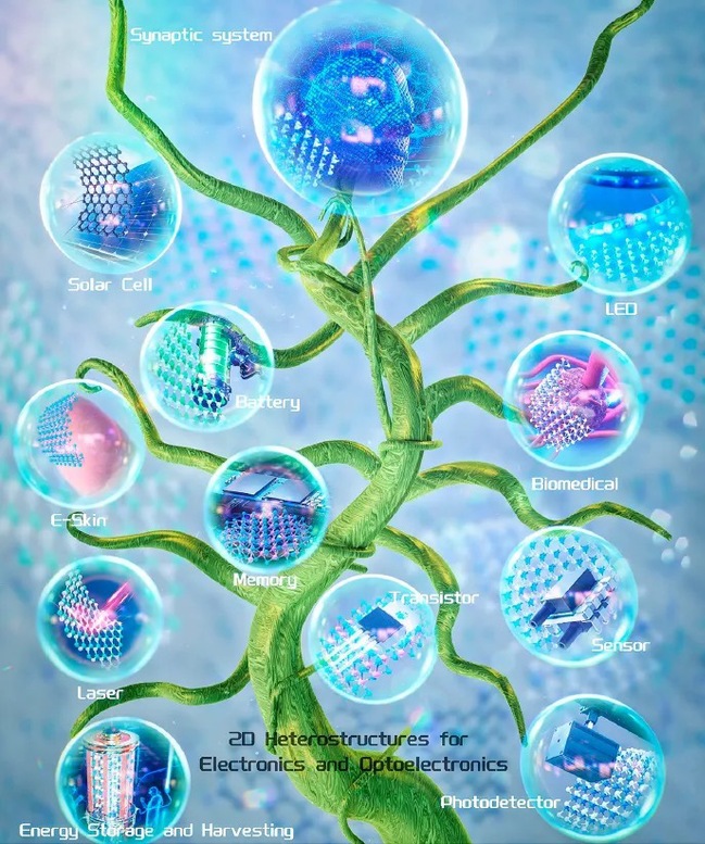
“Grow Tree” based on van der Waals 2D heterostructure devices
More importantly, it is an international co-authored paper. Thanks to the Future Science Research Institute of ZJU-Hangzhou Global Scientific and Technological Innovation Center, the UCLA team of America. Special thanks to National Natural Science Foundation of China and the Fundamental Research Fund for the Universities Affiliated to Chinese Central Government
Link to the paper:https://pubs.acs.org/doi/10.1021/acs.chemrev.1c00735